Applications :
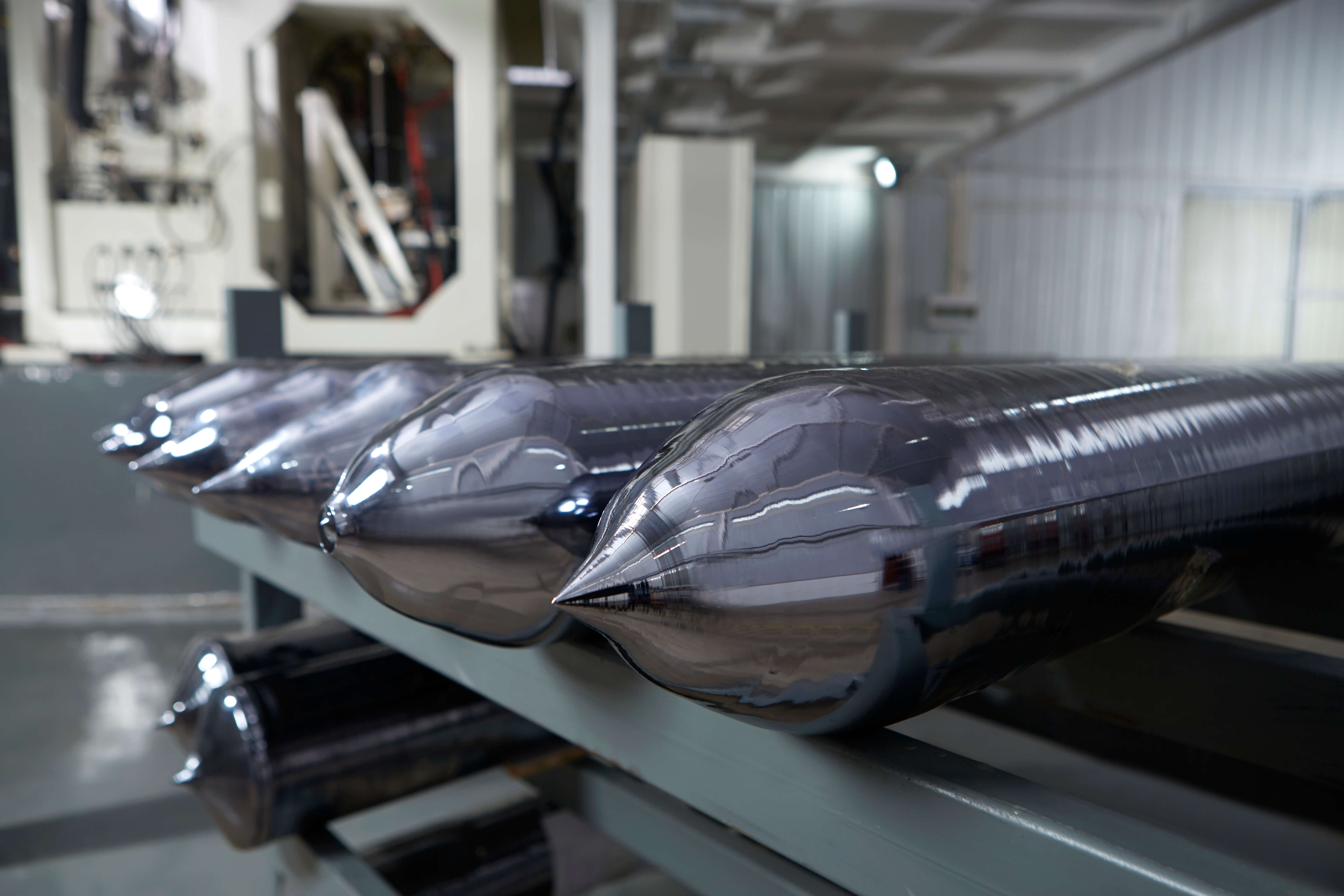
Structure: Mono crystalline
Growing method: CZ/FZ
Type: N/P
Orientation: <111> <100> <110>
Resistivity: 0.05-10000ohm.cm
Grade: Optical/Mirror/Semiconductor/Tar get
Dislocation density: None
Density: 2.33g/cm3
Melting Point : 1414℃
Transmission range: 1.2-15um
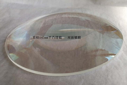
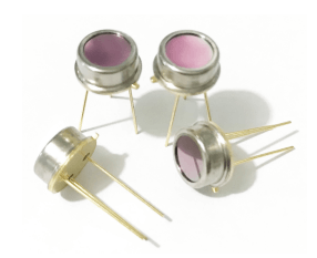
Optical application:band pass filter, thermography, ATR crystal, mirrors,wafer,windows,lenses,ban d pass filter, ATR crystals,etc.
Product Advantage :
ICC has the single-wire cuting machine, multi-wire sawing machine and NC cuting machine.
ICC has more than 20 sets polishing machines for silicon wafers and other windows.
ICC has two sets of Ultrasonic cleaning, and the workers wear cleanroom suits to protect the cleaness and particles.
Product Parameters :
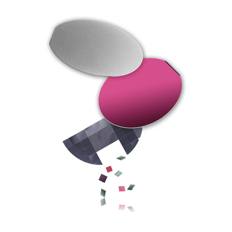
Intrinsic Crystal Technology, provides standard wafers for the semiconductor industry, optical filters, and IC silicon dioxide.
A. Standard Dimensions: 2 inches, 3 inches, 4 inches, 5 inches, 6 inches, 8 inches, 12 inches (300 mm)
B. Resistivity and use – Whether it is SEMI /IC/FILTER grade
C. Polishing requirements: Surface quality of monocrystal silicon polishes: no channel, no erosion pits, no fog, no regional contamination, no edge breakage, no cracks, no pits, no trenches, no mounds, no knife marks, etc.No area stain, no edge collapse, no crack, no knife mark on the back.
thickness (T), 200-1200 um
total thickness variation (TTV) < 10 um
bending (BOW) < 35 um
WARP degrees (WARP) < 35 um
grinding chengdu: SSP/DSP/lap
resistance range: the smaller the price more expensive,
size range: more is not a standard range prices more expensive
crystal direction: “100”, “111” “110”, if you need reference surface
roughness: standard is less than 0.5 nm
flatness: standard is less than 3 um
D. Oxidation treatment: 50nm ~6000nm (routine: 100nm, 200nm, 300nm, 500nm, 1000nm)
products and services.


